WE IGNITESILICON MINDSEVERYWHERE.
End-to-end semiconductor design expertise from architecture to GDSII and post-silicon validation. Engineered for first-pass success.

Our Mission
Engineered for First-Pass Success
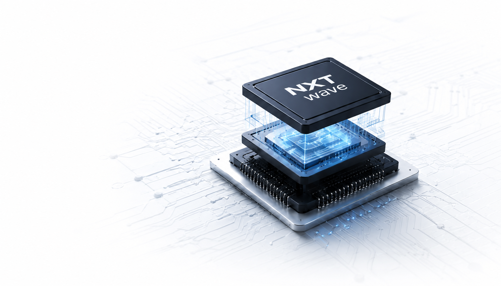
NXTwave Semiconductor is a premier VLSI design firm headquartered in Bengaluru. We provide comprehensive, end-to-end semiconductor design solutions from RTL to GDSII. Our service portfolio spans architectural definition, RTL design, functional verification, synthesis, physical design, DFT, and post-silicon validation.
We partner with fabless design houses and internal chip design teams to achieve first-pass silicon success, driven by our deep domain expertise, rigorous verification, and quality-focused engineering philosophy.
Our Core Strengths
Deep VLSI Expertise
Our team brings decades of combined experience across RTL design, Functional verification, DFT and Physical Design & Verification. This depth of expertise ensures your silicon architecture is built on a solid foundation from day one, reducing costly redesigns and accelerating design closure.
Quality-First Approach
Quality is embedded into every stage of our design flow. Through rigorous testing, validation, and sign-off checks at each milestone, we minimize risk and maximize first-pass silicon success and yield.
Flexible Engagement Models
We understand that every project has different needs. Whether you require full turnkey project development or a focused technical partnership for a specific design phase, we tailor our engagement model to fit your goals, timeline, and budget.
Faster Time-to-Market
By leveraging industry-leading EDA tools and optimized, proven workflows, we help you accelerate your silicon development cycle — without ever compromising on technical excellence or reliability.
Our Core Capabilities
The Complete Silicon Engineering Spectrum
Accelerating time-to-market by integrating seamless RTL-to-GDSII workflows with rigorous technical precision.
Silicon Architecture & Digital Front-End
- RTL Microarchitecture Development (SystemVerilog, VHDL, Chisel)
- SoC / Subsystem Integration & Multi-Clock Domain Management (CDC, LINT)
- Low-Power Architecture Implementation (UPF/CPF, Power-Aware Design)
- Protocol IP Integration (PCIe Gen5/6, USB 4, Ethernet, CXL, LPDDR5)
Functional Verification & Emulation
- Advanced UVM/SystemVerilog Testbench Architecture & Assertion-Based Verification
- Hardware Emulation & FPGA Prototyping (Palladium, ZeBu, Zynq UltraScale)
- Gate-Level Simulation (GLS) & Power-Aware Verification
- Formal Verification & Property Checking (JasperGold / VC Formal)
Physical Implementation & Sign-off
- Sub-5nm Hierarchical & Flat Floorplanning, Placement & Route (Innovus / ICC2)
- Multi-Corner Multi-Mode (MCMM) Timing Closure & Static Timing Analysis (PrimeTime)
- Design for Testability (DFT: ATPG, MBIST, BSCAN, JTAG) & Fault Coverage
- Physical Verification (DRC, LVS, Antenna) & IR/EM Drop Power Integrity Sign-off
Analog & Mixed-Signal (AMS)
- High-Speed Data Converters (ADC/DAC) & Power Management ICs (PMIC)
- Precision Custom Layout & AMS Co-Simulation (Verilog-AMS / RNM)
- SerDes PHY & High-Frequency RF Transceiver Design
- Standard Cell Library & Custom Memory Layout Optimization
Silicon Prototyping & System Board
- High-Density Multilayer PCB Design & High-Speed Signal Integrity (SI/PI) Analysis
- Hardware/Software Partitioning & Pre-Silicon Firmware Bring-up
- Custom FPGA Retargeting & Glue-Logic Acceleration
- Multi-GHz Differential Routing & EMI/EMC Compliance Verification
Post-Silicon Validation & Production
- Silicon Bring-up, Characterization & Voltage/Temperature Stress Testing
- Automated Test Equipment (ATE) Program Development & Wafer Sort
- Root-Cause Failure Analysis (SEM / FIB Diagnostics)
- Production Yield Optimization & Reliability Qualification
Industries We Serve
Automotive ICs
Compute, Safety, High-Integrity Systems
AI / ML Accelerators
High-Performance Compute, NPU, GPU
5G / RF Systems
RFIC, mmWave, Connectivity
IoT Solutions
Low-Power, Secure, Connected Devices
Industrial Edge
Edge Computing, Control, Automation
Medical & Biotech
Precision Systems, Embedded Electronics
Careers
Build the Future of Silicon
Our engineering process transforms complex silicon innovation from concept to chip.
- 01
REVIEW
Technical assessment by our lead architects.
- 02
DEEP-DIVE
Architecture and verification discussions.
- 03
DELIVER
Fast-track integration into our engineering nodes.
Let's Build What's Next.
Have a project in mind? Let's build the extraordinary together — from first concept to production silicon.
Get in Touch